
4. 프로세서 개념과 설계
4장 프로세서 개념과 설계 개요
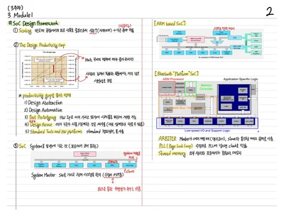
프로세서(Processor) 는 명령어를 실행하는 SoC의 두뇌. 본 장에서는 프로세서의 기본 구성, 처리 단계, 명령어 추상화, ISA, Core와 Processor의 차이를 정리한다.
프로세서란?
- 명령어를 수행해 일정한 연산을 수행하는 HW
- 필요한 자원: Register, ALU, Control unit, Memory interface
프로세서의 처리 단계
- Fetch: Memory에서 명령어(Instruction)을 읽어옴
- Decode: 명령어를 해석
- Execute: ALU 연산, 데이터 처리
- Memory Access: Load/Store
- Write Back: Register에 결과 저장
프로그래머의 관점
Level of Abstraction (추상화 계층)
- High-level language: C, Python, Java
- Assembly language: 기계어에 가까운 상징적 표현
- Binary machine code: 0/1 비트 스트림
→ Compiler는 high-level을 assembly로, Assembler는 assembly를 binary로 변환.
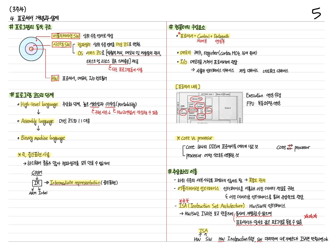
Core vs Processor
- Core: Processor의 핵심 계산 장치 (ALU + Register + Control)
- Processor: Core + Cache + Memory controller + I/O interface
예: ARM Cortex-M0 Core을 라이선스해서 만든 Processor (SoC) = STM32F103 등. Core 설계는 ARM이, 주변 IP는 각 vendor가.
Core의 예
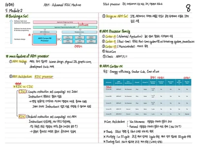
- ARM Cortex-A/R/M series
- ARM Cortex-M0/M3/M4 — Cortex-M family
추상화 레벨
- Microarchitecture: 파이프라인, 캐시, branch predictor 등 구현 세부사항
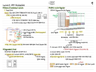
- ISA (Instruction Set Architecture): 명령어 집합, register, memory model. 프로그래머에게 노출되는 인터페이스
같은 ISA(ARMv7-M)를 구현하는 여러 microarchitecture 존재 → Cortex-M3, M4, M7 등.
프로세서 설계 흐름
- ISA 결정: ARM, RISC-V, MIPS, x86, …
- Microarchitecture 설계: 파이프라인 단계, branch prediction, cache 구조
- RTL 기술: Verilog/VHDL로 구현
- Synthesis: Gate-level netlist로 변환
- Place & Route: 레이아웃
- Fab: 웨이퍼 제조
ARM Cortex 패밀리
- Cortex-A (Application): 고성능, Linux/Android 용 (iPhone, Raspberry Pi)
- Cortex-R (Real-time): 실시간, 자동차/HDD (deterministic latency)
- Cortex-M (MCU): 저전력 MCU (STM32, nRF52)
Cortex-M 세부
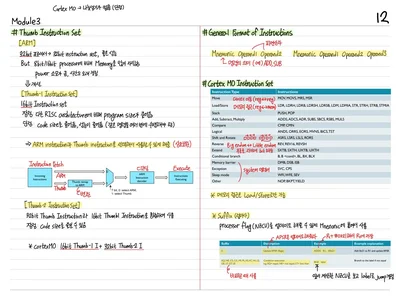
- M0/M0+: 초저전력, ARMv6-M (Thumb만)
- M3: ARMv7-M (Thumb-2)
- M4: M3 + DSP/FPU
- M7: 고성능 MCU
프로세서 설계의 트레이드오프
- Performance: clock frequency, IPC (instructions per cycle)
- Power: static + dynamic
- Area: 실리콘 면적
- Verification: 검증 복잡도
Cortex-M0는 11k gates로 초소형 → 저가 MCU에 적합, Cortex-A72는 수백만 gate로 고성능 → 스마트폰 AP.
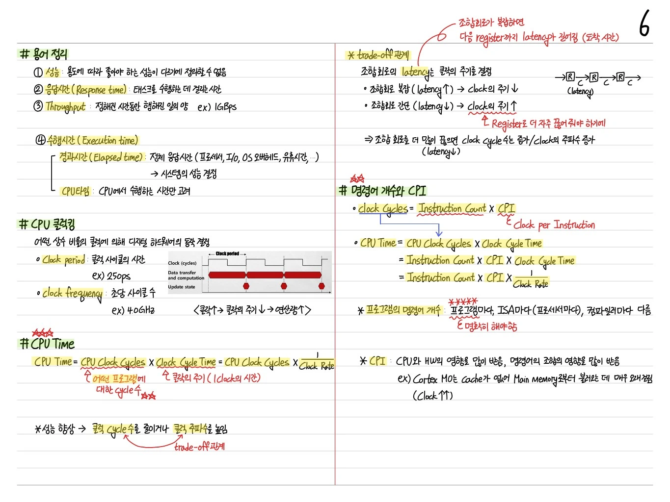
ISA 예
- ARM: RISC, fixed-length, load/store
- Thumb/Thumb-2: ARM 축약 16-bit, 코드 공간 절감
- x86: CISC, variable-length
- RISC-V: open-source RISC, 확장 가능
ARM은 load/store architecture → 메모리 접근은 LDR/STR로만, 연산은 register 간에만.
예제: ADD 명령어 실행
ADD r0, r1, r2
- Fetch: PC에서 명령어 binary 읽음 (
0xE0810002) - Decode: opcode=ADD, Rd=r0, Rn=r1, Rm=r2 해석
- Execute: ALU가 r1 + r2 계산
- Write Back: 결과를 r0에 저장
- PC += 4: 다음 명령어
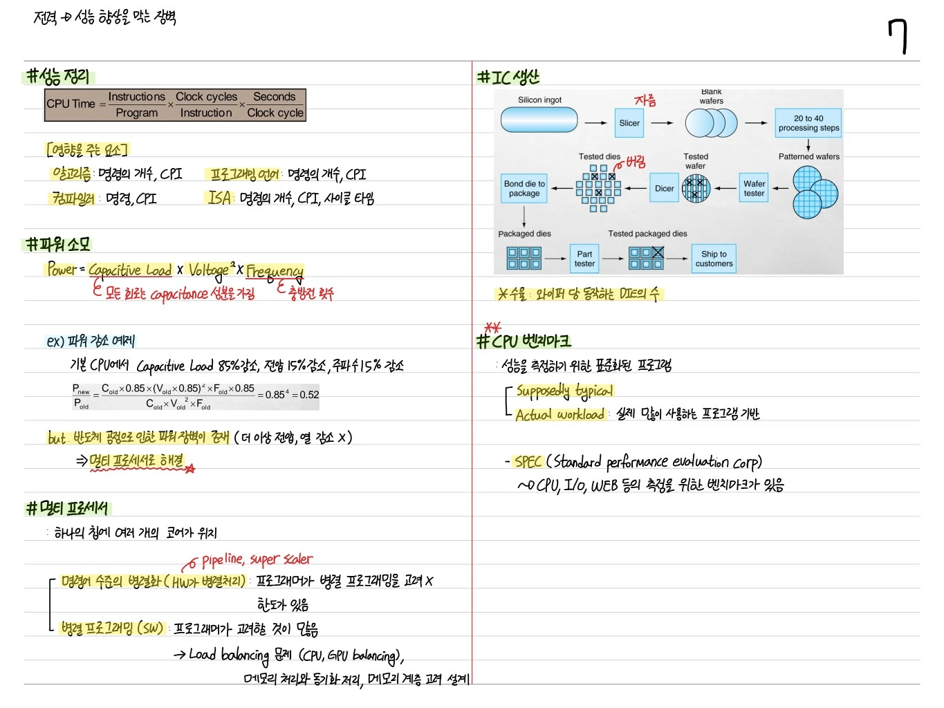
정리
| 개념 | 설명 |
|---|---|
| 처리 단계 | Fetch → Decode → Execute → Memory → Write-back |
| Core vs Processor | Core ALU+Reg+Control, Processor Core + 주변 |
| ISA | 프로그래머 인터페이스 (ARM, x86, RISC-V) |
| Microarchitecture | ISA 구현 방법 (파이프라인, 캐시) |
| Abstraction | HLL → Assembly → Binary |
프로세서는 ISA와 Microarchitecture라는 두 축으로 진화하며, SoC 설계자는 필요한 Core IP를 라이선스해 전체 시스템에 통합한다.
 SoC Note
 AI Study Note
 Embedded Note
Comments (0)
No comments yet. Be the first to comment!
Please to write a comment.